SECONDMENT
PHOTONICS STRUCTURES INTEGRATED ON CHIPS OR FIBERED IN INNOVATIVE MATERIALS
FROM : UNIVERSITÉ DE BORDEAUX (FRANCE)TO : UNIVERSITÉ LAVAL (QUÉBEC)
FROM : 2 DECEMBER 2019 TO : 3 APRIL 2021
Involved Work Packages :
![]()
![]()
![]()
RESEARCHER

OBJECTIVES
The objective of this secondment is to design and manufacture complex photonic structures, integrated on chips or fibered in innovative materials, for photonics in complex environments. Conversely, optical approaches in complex environments will be used to propose new laser structuring methods.
Controlling wave transport in complex environments has been a highly multidisciplinary, active and dynamic field of research since the mid-1990s. The fundamental study of the mesoscopic aspects of wave propagation, particularly of light, has thus enabled the development of many applications in imaging and information processing. The usual approaches consist in shaping the wavefront, in a controlled way, in order to focus the light through a scattering medium (Fig. 1a), for example, or in manufacturing an artificial complex medium in such a way that the light spreads there according to a pre-established pattern (Fig. 1b).
Recent theoretical advances combined with technological advances in the manufacture of optical materials and the development of new structuring tools at the micro and nanometric scale allow new types of complex media to be explored. Among innovative media, structured materials with a non-linear optical response have shown increasing interest in recent years. They are still poorly studied in the field of photonics in complex environments and naturally have a strong application potential.
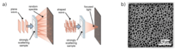
Figure 1.
TASKS
A1 – Non-linear nanocomposite waveguides, WP3
A2 – Non-linear optical fibers printed in 3D, WP4
A3 – Laser post-manufacturing of photonic components on LiNbO3, WP4
A4 – Laser structuring in diffusing media, WP3
RESULTS
Modelling of laser inscribed directional couplers operating in the MIR
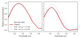
The development of coherent sources and other optical components for the mid-infrared has been hampered by the lack of sturdy materials that can withstand high power radiation or exposition to harsh environment. BGG glasses are robust materials transmitting over the 2.5–5 μm region. We report in this work the direct femtosecond laser fabrication of efficient directional couplers integrated in a BGG glass chip. The photonic components are characterized from 2.1 to 4.2 μm and compared to similar structures inscribed in silica glass samples. At 2.85 μm, a 99% relative cross transmission is reported in BGG glass. The experimental measurements are in good agreement with the coupled mode theory (CMT) for wavelengths up to 3.5 μm.
The directional coupler system under investigation is sketched in Fig. 2a and modeled, using a phenomenological approach, in Fig. 2b. Considering each waveguide with a circular cross section, the power cross transmission can be analytically expressed.
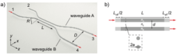
Figure 2. (a) Schematic of the directional coupler composed of two evanescently coupled waveguides A and B. Both input ports (1 and 2) and output ports (3 and 4) are separated by a distance D. They are brought close via S-bend parts (with curvature radius R) and interact over a straight segment L. In the coupling region, waveguides are separated by a distance d. (b) Simplified model of the directional coupler composed of two circular step-index waveguides. The S-bend parts are modeled by a straight part with effective length Leff.
Figure 3 shows directional coupler transmission measured at 2.85 µm in BGG (a) and silica (b) glasses. An efficient tranmission (~99%) is obtained in the BGG glass. Using the previous equation, a fitting procedure is applied to extract the parameters and Leff. These parameters are then included in the CMT equations and the obtained numerical simulations are in very good accordance with the experimental data (sahed blue lines).
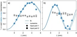
Figure 3. Total transmission (gray markers) and relative cross transmission (blue markers and lines) of directional couplers with varying interaction length L for BGG (a) and fused silica (b). The measurement is performed at 2.85 𝜇m. Full circles (resp. squares) correspond to input power in port 1 (resp. port 2). The blue line is the fit based on the equation in the text. The fit parameters are 𝜅=0.29 mm−1, Δ𝑛eff=0.35×10⁻⁴ and 𝐿eff=1.70 mm for BGG and 𝜅=0.51 mm−1, Δ𝑛eff=1.57×10⁻⁴ and 𝐿eff=1.89 mm for silica (see text for details). The blue dashed lines are numerical results obtained from the coupled mode theory equations for straight directional couplers with circular step-index waveguides. The radius 𝑎 = 10.6 𝜇m (resp. 7.25 𝜇m) and the separation 𝑑= 25 𝜇m (resp. 20 𝜇m) correspond to the experimental configuration for BGG (resp. silica). The coupler effective length 𝐿eff and the detuning Δ𝑛eff correspond to the fit parameters.
Similar numerical simulations are also used to study the broadband transmission in the BGG glass (see Fig. 4). Although coupled-mode theory seems well suited to model the directional coupler behavior up to 3.5 𝜇m, it clearly fails for larger wavelength. Additionnal FDTD simulations suggests that the normal-mode theory rather than the CMT should be considered to properly model our device at large wavelengths.